AI is rapidly becoming one of the largest infrastructure asset classes in the world. But the physical asset at the heart of that infrastructure, the AI chip, has not yet accumulated years of reliability data, standardized useful-life assumptions and residual-value history that lenders take for granted in mature infrastructure asset classes.
While AI chips are a major (expense) component, AI data center financing today relies heavily on contracted cash flows, customer credit, and broader project economics rather than on long-duration residual-value assumptions for the AI chips themselves. The AI chips themselves are often given no collateral value.
It is time for AI chips themselves to be bankable.
Diamond Foundry (DF) is helping make AI chips bankable with new Single Crystal Diamond (SCD) substrated chip packaging that addresses one of the most important controllable accelerants of chip speed and semiconductor degradation and performance loss.
SCD substrating increases the thermal envelope of a chip which chip designers can choose to translate either into faster speed, higher lifetime, or any combination thereof – in all cases boosting lifetime tokens per dollar of capital invested. The fundamental financing unit of AI infrastructure is less so the GPU; it is lifetime useful compute, or lifetime tokens, produced per dollar of capital invested. If a $30,000 accelerator can reliably produce useful compute for six years rather than two or three, its lifetime economics change dramatically. So does the amount of debt that can rationally be placed against the infrastructure, i.e. AI chips made bankable.
From a Computing Product to an Infrastructure Asset
The GPU has undergone an extraordinary transition. GPUs originated as processors for graphics and gaming workloads. They evolved into massively parallel computing devices and ultimately became the computational foundation of modern AI. Today, descendants of that architecture are being deployed by the hundreds of thousands in multi-billion-dollar data centers and operated at extremely high utilization for years.
The financial expectations placed on the hardware have therefore changed just as dramatically as the workloads. AI accelerators are increasingly expected to behave not merely like computing equipment, but like infrastructure assets.
Other industries have gone through similar transitions. Early photovoltaic technology was not automatically suitable for a utility-scale solar project financed against 30 years of expected cash flows. Solar became a bankable infrastructure asset through enormous engineering effort around degradation, thermal cycling, packaging, qualification, warranties and field-performance data. The same happened with turbines, aircraft engines and power electronics.
Reliability and value engineering convert technology into infrastructure. AI is now beginning that transition. And it starts with the biggest lever – peak temperatures.
The Financing Market Is Already Exposing the Problem
AI infrastructure can certainly be financed today. But financing structures reveal how young the asset class remains. For example, CoreWeave has completed billions of dollars of HPC infrastructure-backed financings, including an $8.5 billion investment-grade facility backed by HPC infrastructure together with an associated customer contract. The significance is not that GPUs have no collateral value. They clearly do.
The significance is that lenders are still learning how to value the combination of GPU useful life, technological obsolescence, residual value, customer contracts and infrastructure reliability over multi-year financing periods.
Even accounting assumptions remain controversial. Michael Burry has argued that hyperscalers are extending the accounting lives of computing equipment beyond what their rapid product cycles justify, estimating that depreciation could consequently be understated by approximately $176 billion between 2026 and 2028.
Whether or not Burry’s estimate ultimately proves correct, the debate identifies a fundamental question for the AI infrastructure industry: What is the economically useful life of an AI accelerator operated continuously with temperatures constantly reaching the spec maximum?
Peak Temperature Is a Key Driver
Semiconductor reliability is strongly temperature dependent. Elevated local temperatures accelerate multiple physical degradation mechanisms, including electromigration, interconnect degradation, dielectric breakdown and thermomechanical fatigue (e.g. TI reliability calculator).
And the relevant thermal problem is not simply average chip temperature. It is local peak temperature.
Modern AI processors do not dissipate heat uniformly. Very high activity occurs in localized regions of the silicon, producing transient and sustained hotspots whose local power density can substantially exceed the chip-wide average.
For high-power training accelerators, these hotspots can occur around heavily utilized tensor-compute and associated data-movement structures.
In more highly parallel inference architectures, smaller computational and memory structures – including static random-access memory (SRAM) and multiply-accumulate (MAC) regions – can create still smaller hotspots with extremely high local heat flux.
Consequently, a cooling system can maintain an apparently acceptable average die temperature while microscopic regions of the silicon and interconnect stack experience substantially harsher thermal conditions. That distinction matters because semiconductor degradation is nonlinear with temperature (NIST).
Average temperature does not determine lifetime; the hottest parts of the chip disproportionately do.
SCD Substrated Chips
Diamond Foundry’s SCD substrate attacks peak temperature and addresses this problem at the chip level.
SCD’s stand-out thermal conductivity allows heat generated in microscopic regions of the active silicon to spread laterally before entering the chip package and the cooling system.
SCD substrating enhances a chip’s thermal envelope in two ways: it flattens the frontside hotspots; and it boosts backside cooling capacity by virtue of the “bandwidth” (area) then being higher for downstream thermal flux through downstream thermal resistors.
The objective is not simply to reduce the average temperature of the AI chips. It is to compress the temperature distribution across the die – shaving the peaks; and then to enable downstream cooling to work more efficiently.
Chip designers can use the enhanced thermal envelope of a chip in two ways:
Increase Performance: run the chip at higher frequency, power, or dynamic utilization while remaining within an acceptable thermal envelope.
Increase Lifetime: maintain the performance while reducing hotspot temperature and therefore slowing temperature-accelerated degradation mechanisms.
Or the benefit can be divided between the two.
Either way drives lifetime tokens per capital invested.
SCD substrating means Chip Hotspots, Gone.
From Peak Temperature to Bankability
Standard semiconductor reliability models show strong temperature dependence for multiple wear-out mechanisms. For an illustrative failure mechanism with a 0.7 eV activation energy, reducing a sustained hotspot from 95°C to 80°C corresponds to approximately a 2.5–3× improvement in the temperature-driven lifetime of that particular mechanism.
Peak temperatures found in chips are very bad for chips. They accelerate a plethora of chip failure mechanisms. That does not mean that reducing hotspot temperature automatically triples the lifetime of an entire GPU. GPU lifetime depends on many components and failure mechanisms. It does mean that temperature is an unusually powerful and engineerable reliability variable.
Learn more in Hotspots are Evil and Hotspots are Everywhere
AI Data Center Economics
AI data centers are capital intensive. A large portion of data center investment scales with the number of accelerator packages deployed: GPUs or ASICs, HBM, networking equipment, boards and related systems. Another portion scales more directly with electrical power and facility infrastructure.
Actual savings will depend on how a specific processor converts thermal headroom into performance and extended lifetime. Memory bandwidth, interconnect, power delivery, voltage-frequency scaling, workload and software utilization can all become limiting factors.
From FLOPS per Watt to Bankable Lifetime Tokens per Capex
The AI industry currently focuses heavily on instantaneous metrics: FLOPS per watt. Tokens per second. Rack density. Power per GPU. Those metrics matter but infrastructure finance ultimately cares about a different quantity: Bankable lifetime tokens per dollar of capex.
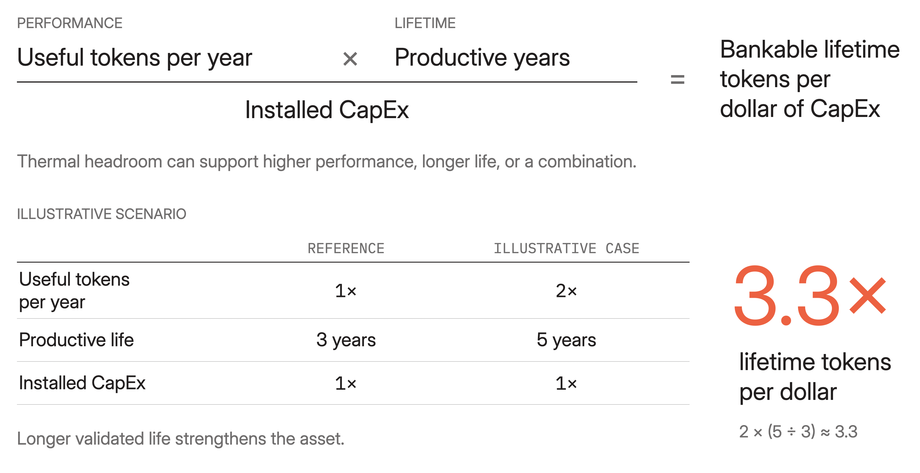
Lifetime tokens per installed CapEx: useful tokens per year × productive years ÷ installed CapEx.
An AI chip that produces 20% more tokens per second but has a materially shorter useful life may be economically inferior to one producing somewhat less instantaneous performance but operating reliably for substantially longer.
Conversely, a processor whose hotspot temperatures can be reduced sufficiently to extend its useful operating life – or whose thermal headroom permits additional useful compute without sacrificing reliability – can generate substantially greater lifetime compute from the same semiconductor capital.
This creates a new way to think about how we help convert AI accelerators from rapidly depreciating computing equipment into more bankable infrastructure assets. The solar industry had to engineer photovoltaic modules capable of surviving decades in the field. The aviation industry had to engineer engines around predictable maintenance intervals and component lifetimes. AI infrastructure will increasingly have to engineer accelerators around predictable multi-year useful lives. We believe better thermal chip packaging will be key to it.
At Diamond Foundry, we are excited to help provide one of the physical building blocks for doing that.
The problem is not merely watts per chip. It is peak watts per square millimeter, peak temperature, and the cumulative damage those peaks produce over years of operation. And ultimately the financial metric is not the purchase price of the GPU. The metric is bankable lifetime tokens per dollar of capital invested.