Hotspots are evil. And hotspots show up across chip architectures. They are surely abundant in high-power training GPUs/TPUs. But perhaps surprisingly to some, they show in seemingly cooler low-voltage inference chips where hotspots can even have higher peak power densities than in high-power chips. They are well known to constrain networking chips, power electronics, etc.
Training GPUs and TPUs increasingly combine very large compute dies with package powers approaching or exceeding the limits of conventional cooling architectures. Their localized compute regions can operate at substantially higher heat flux than package-average power density suggests.
But lower-voltage inference architectures do not eliminate the problem. Lower voltage can substantially reduce energy per operation, enabling architectures that substitute greater parallelism and silicon area for frequency. Yet compute, SRAM, network-on-chip and power-delivery activity remain spatially non-uniform. Smaller regions can therefore dissipate less absolute power while still producing extremely high local heat flux.
Lower-power devices can therefore be cooler on average while still containing intense microscopic hotspots. This distinction between average chip power and peak local power density is central to DF’s opportunity.
High-Power AI Training Chips
The raw power constraint is particularly evident with AI training processors. Current roadmaps for AI training chips present significant thermal management challenges on total power alone.
AI chip companies like NVIDIA project thermal design power (TDP) well above 1,000W with compute chiplets close to the reticle limit (33 × 26 mm). Add to this even larger packages, like large CoWoS/SoIC or SoW-X packages with a TDP exceeding 15,000W.
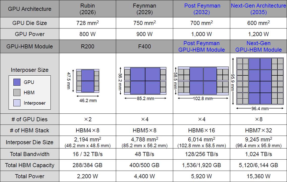
Chiplet level power densities range from 100 to 200W/cm2 with hotspot power densities exceeding 1,000W/cm2.
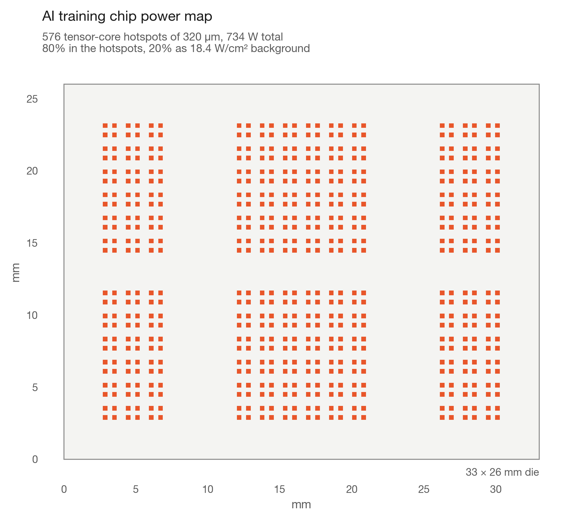
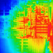
Thermal model of a high-power AI training chip’s thermal map: 572 tensor-core hotspots of about 1 W each on a 33 × 26 mm die.
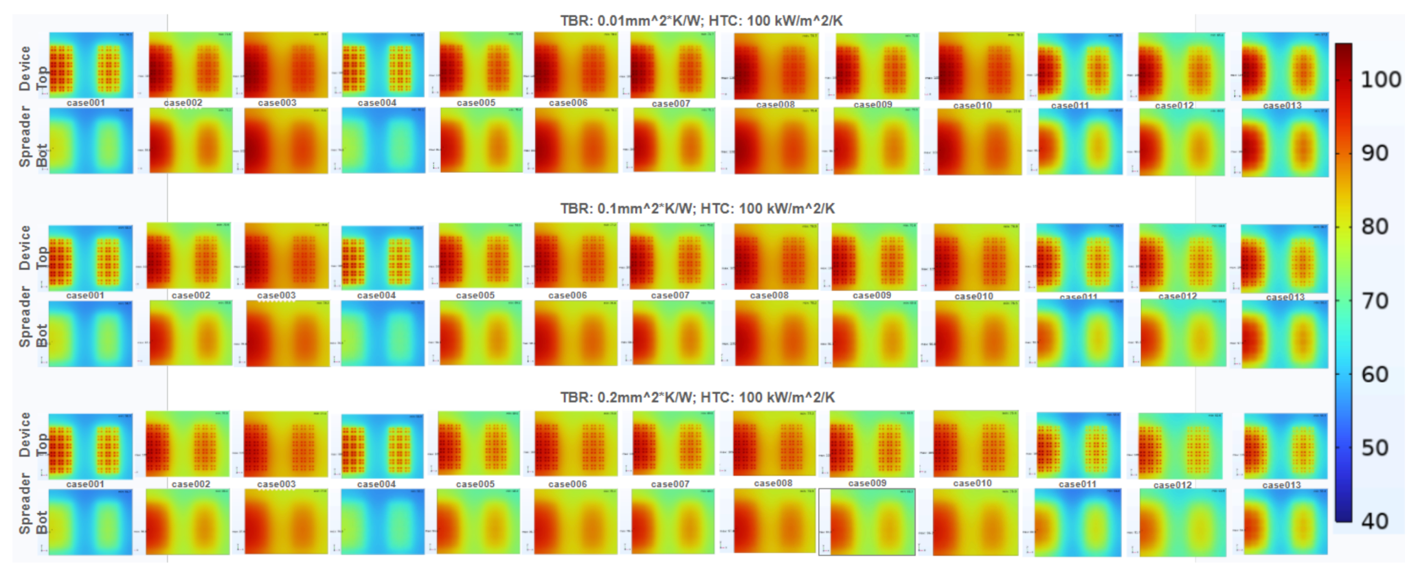
Modeled training-chip temperature maps comparing direct cooling and a heat spreader across workload cases and thermal boundary resistance settings.
Much of the root cause of such hotspots lies in the silicon material used for making transistors – in particular the thick passive silicon layer below the transistors. When silicon is thinned for Single Crystal Diamond (SCD) substrating and SCD is bonded close to the active layer, localized heat can reach the SCD while significant spatial non-uniformity still remains. The SCD can then perform the lateral heat-spreading function near the point where it is most valuable.
Lower-Voltage AI Inference Chips
AI inference processors feature extremely high peak power densities even though the entire chip is lower power and seemingly cooler.
High-throughput inference benefits from lower-voltage, more highly parallel architectures in which additional silicon area substitutes for frequency. Because dynamic power falls approximately with the square of voltage, such architectures can materially improve energy efficiency. Lower average power density, however, does not per se produce a uniform thermal map.
AI processors combine ASML reticle-limit size compute dies, dense matrix-multiplication engines, SRAM, network-on-chip infrastructure, power delivery and increasingly complex advanced packaging. These functions do not consume power uniformly. Instead, they generate small, rapidly changing regions of high heat flux that can operate tens of degrees hotter than neighboring regions. Local memory must remain physically close to the arithmetic units it feeds because repeatedly moving operands over long distances consumes substantial energy.
The result is an accelerator composed of many localized compute-and-memory regions rather than a completely homogeneous sea of power.
Illustratively, this means a transition from relatively large (e.g. 300 µm), high-power (e.g. 1W) hotspots toward smaller (e.g. 50 µm) hotspots operating at lower absolute power (e.g. 0.05W). It turns out the power of the low-power hotspot is less of a factor smaller than its area size: 1W/(300 µm)² ≈ 11 W/mm² whereas 0.05W/(50 µm)² = 20 W/mm², so this low-power hotspot actually produces even higher local heat flux.
The implication is important: a future low-voltage accelerator can look relatively cool when measured by total TDP or average W/mm². But it still contains large numbers of localized thermal peaks that constrain junction temperature, clock frequency, and sustained performance and reliability. And the relevant thermal limitation for chips is max hotspot temperature and this is driven by peak power density.
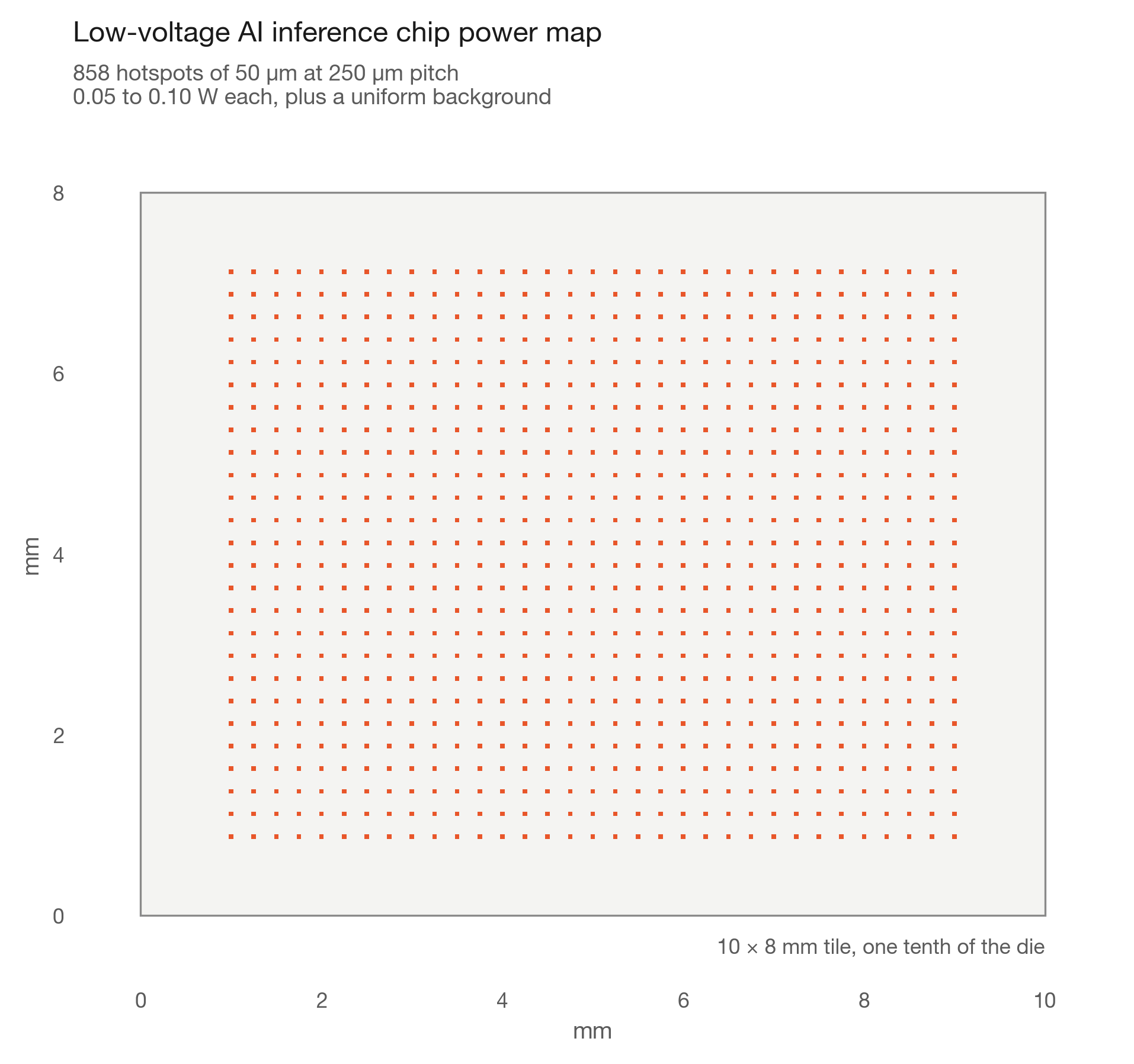
Thermal model of a low-voltage AI inference chip’s power map: More than 10,000 hotspots, each 50 µm wide at 250 µm pitch with hotspot power ranging from 0.05 to 0.10 W. 10 × 8 mm sub-region shown.
Low-voltage design therefore creates two possible outcomes. One is to use lower voltage to reduce total system power and leave the resulting thermal headroom unused. The other is to reinvest some of that headroom into greater simultaneous activity, additional compute density, higher utilization or selectively higher frequency.
Semiconductor economics have historically provided a strong incentive to convert available process, power and thermal capability into additional performance. SCD is compatible with either architectural direction. Its economic value will be highest in devices where local heat flux or thermal uniformity continues to constrain useful compute.
Reasoning and Agentic Inference
The evolution from commodity inference toward reasoning and agentic workloads may further increase the value of high sustained performance.
Large portions of transformer computation remain highly parallel. However, complex agentic workloads also introduce synchronization points, repeated reasoning stages, verification, tool invocation and sequential dependencies. Overall task latency can therefore be governed partly by a critical path that cannot simply be eliminated by adding parallel compute.
This creates a potential economic incentive to operate parts of future accelerators over a broader voltage-frequency range: highly energy-efficient low-voltage operation for throughput-oriented phases, combined with selectively higher-performance operating points for latency-sensitive phases.
If thermal constraints limit these operating points, additional near-junction heat spreading can have value even in architectures fundamentally designed around energy efficiency.
DF therefore does not view SCD as a technology dependent on specific AI processor technology. We view it as a component that expands the performance envelope available to chip architects and enables chips to justifiably reach the durability and lifetime required for most economic financial depreciation periods.
Two Decades of Clock Speed Stagnation in CPUs
While the semiconductor industry has steadily increased transistor density at an extraordinary rate, operating frequency and power have stagnated in mainstream CPUs – due to the thermal envelope hitting the power wall:
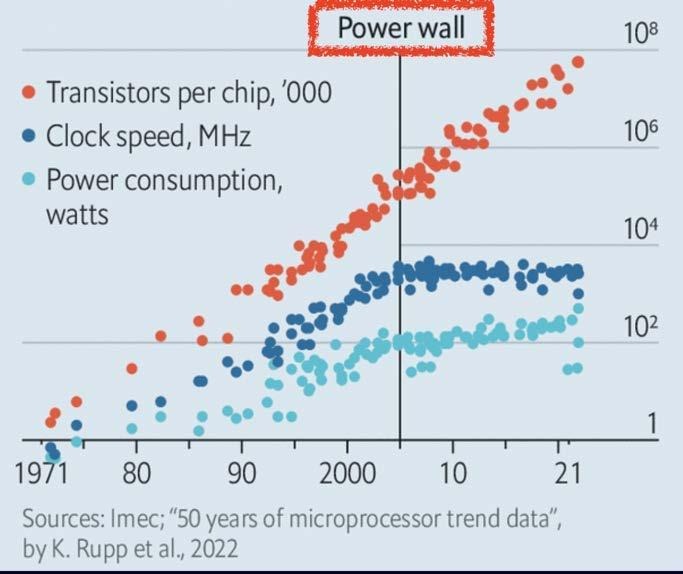
Processor design has stagnated on thermal for two decades now – not for the lack of trying but for the lack of a high-performing material. Designers have had the same old materials to work with for all these years, and these materials are just not very good.
Networking Chips, Power Electronics
High-performance networking chips can also operate at substantial power and feature problematic hotspots. The exact comparison with a GPU depends on the devices and workloads.
Power electronics has heavy, steady hotspots that require de-rating of power modules. DF has demonstrated the doubling of Amps possible in electric-car power modules using DF substrates.
SCD Substrating
Single-crystal diamond (SCD) substrates of ASML reticle-limit size did not exist even two years ago. Now they exist and are available in volume.
The advent of SCD wafers has fundamentally changed what can be done with chips. When our engineers present SCD to veteran thermal chip engineers, they have not seen any such leapfrog opportunity over careers spanning multiple decades.
The architecture can change. SCD substrating is the ultimate technology to achieve Hotspots, Gone.