The material comparison on Bankable AI Chips raises a further question: how much heat can a material carry, in which direction, and how can it be integrated beneath a finished silicon chip? Graphene, polycrystalline diamond, and silicon carbide illustrate the limits of a conductivity-only comparison.
Graphene: conductivity, conductance, and substrate stability
Graphene exhibits exceptional intrinsic in-plane thermal conductivity but its extremely small thickness limits total thermal conductance – and high-power chips require a high level of conductance.
The analogy is a thin copper wire and a thick copper cable both have the same conductivity, that of copper, but the thick cable has much better conductance.
Furthermore, graphene being so thin, it is not suitable as a substrate. A substrate holding a silicon transistor film one third the thickness of a piece of paper must have some extent of mechanical support – it requires some hundreds of microns of thickness at least for a robust material.
Polycrystalline diamond and bonded CMOS
Polycrystalline diamond is commercially established and can be manufactured over large areas.
Somewhat counterintuitively (as it is different with most other materials), polycrystalline diamond is 5× more expensive to produce and also 5× less conductive thermally (vertically) than single-crystalline diamond (SCD).
Only SCD is isotropic. Poly is anisotropic, meaning, it does not conduct equally well in all directions. For hotspot spreading, this is important.
Only SCD can be cost-efficiently polished to wafer precision surface finish. Poly is extremely expensive to polish.
Polycrystalline diamond can be directly deposited to the back of GaN RF chips because GaN can take high temperatures of diamond deposition. However, AI and other silicon CMOS chips cannot take high diamond deposition temperatures, therefore separate bonding is required, in which case customers may as well go for the highest-performing diamond, i.e. SCD.
Silicon carbide: incremental thermal headroom
SiC has significantly higher thermal conductivity than silicon and is available in semiconductor wafer formats in volume. As such, it can provide a benefit over silicon for sure.
SiC’s thermal conductivity, however, remains factors below that of SCD and is furthermore directionally dependent (anisotropic), meaning in-plane and through-plane conductivities differ.
Thermal conductivity
SiC has higher thermal conductivity than silicon but much lower thermal conductivity than SCD.
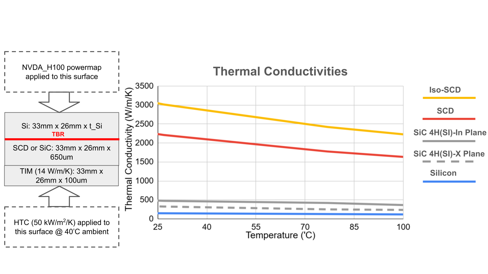
Thermal headroom for one chip generation
SiC can provide a bit of additional thermal headroom relative to plain silicon – say, for one chip generation and for saving stretched thermal requirements only but not to actually extend lifetime and bankability. The smaller thermal envelope available from SiC leaves less room to pursue both greater power and longer life.
Limits of the wafer-size benefit
While SiC is available in 300 mm wafer form matching silicon wafers, wafer-to-wafer bonding faces thermal mismatch challenges. Thermal mismatch grows with differences in thermal expansion coefficient, bonding temperature delta – and substrate size. So using larger wafers is actually harmful from a bonding perspective.
Choosing a substrate for AI chips
For AI chips, the choice comes down to how much heat a substrate can carry and how it can be integrated beneath finished silicon. SCD brings these requirements together: high thermal conductance, heat spreading in every direction, and a surface suited to precision bonding.