Products
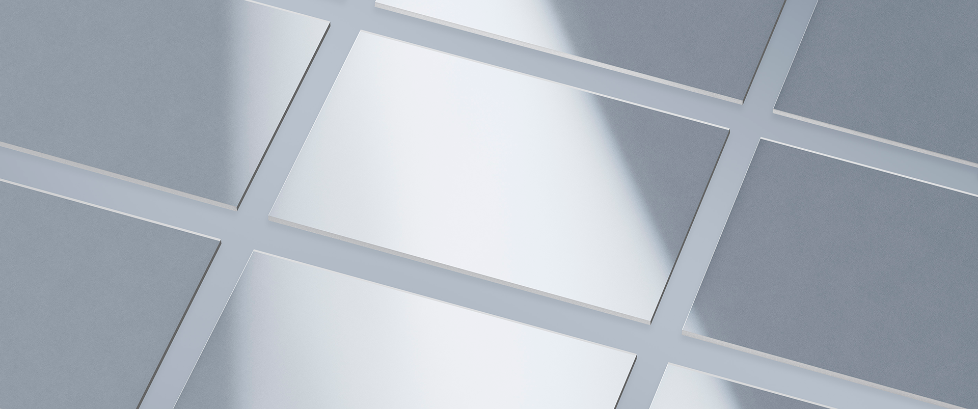
Single Crystal Diamond (SCD) substrates.
New for chip companies
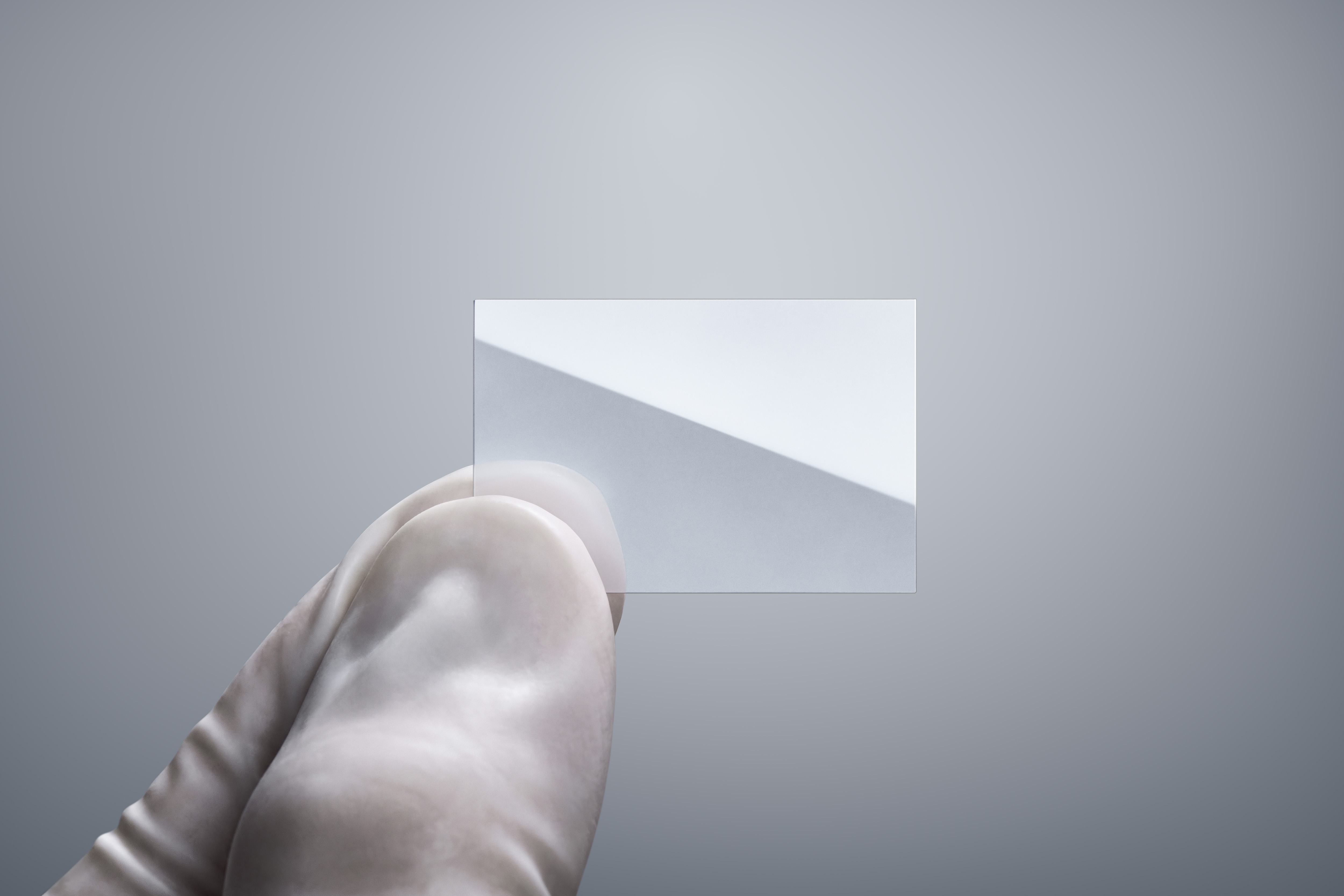
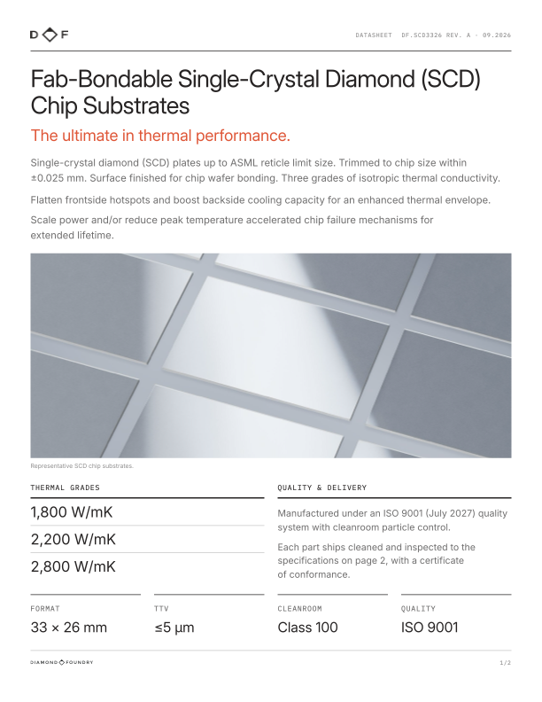
33 × 26 mm SCD Chip Substrate
Single Crystal Diamond plates trimmed to chip size, with the flatness for direct chip wafer bonding. Two thicknesses, three grades of thermal conductivity.
KEY SPECIFICATIONS
Dimensions
33 × 26 mm, ±0.025 mm
Thickness
300 or 650 μm
Thermal conductivity
1,800 / 2,200 / 2,800 W/mK
Thickness variation (TTV)
≤5 μm
Warp
≤5 μm
Ships to qualified chip companies in batches of 25, with a certificate of conformance. Pricing upon request. Orders include a $500 handling fee, which covers our significant overhead for small volumes.
Contact us →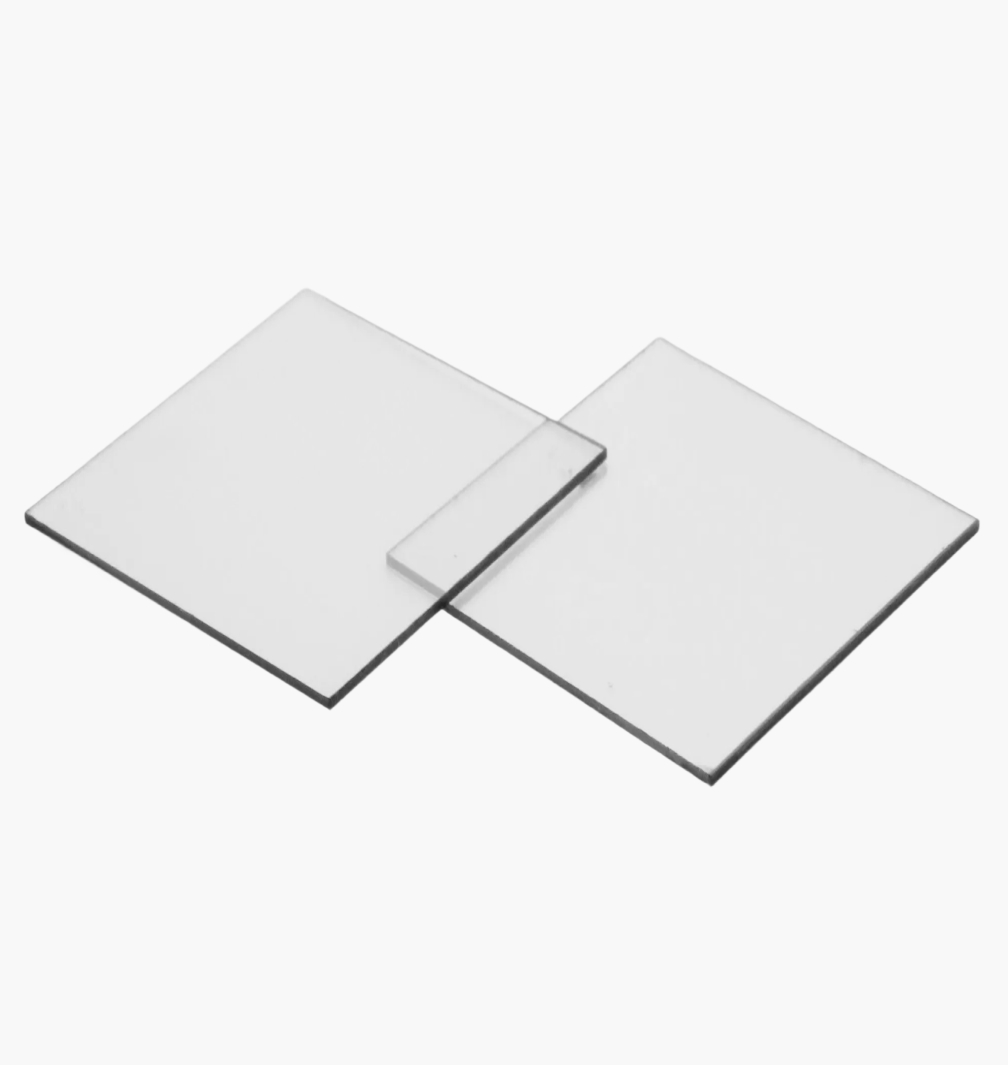
For R&D labs
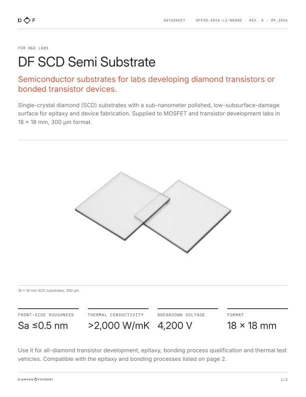
18 × 18 mm SCD Semi Substrate
Single Crystal Diamond sample substrates with a sub-nm polished semiconductor-grade surface and minimal subsurface damage, for all-diamond transistor development and epitaxy.
Semi finish, Sa ≤0.5 nm. Compatible with metallic and direct atomic bonding, including plasma-assisted fusion bonding and surface-activated bonding.
KEY SPECIFICATIONS
Dimensions
18 × 18 mm, ±0.050 mm
Thickness
300 μm, ±25 μm
Thermal conductivity
2,200 W/mK at room temperature
Thickness variation (TTV)
≤5 μm
Breakdown voltage
4,200 V
Price per unit
$23
Bundle of 5 · $115
Orders in five-unit bundles include a $500 handling fee, which covers our significant overhead for small volumes.
Volume pricing, wafer sizes and custom formats.
Custom thicknesses, sizes and surface finishes are available in R&D quantities.
Sale subject to Diamond Foundry Terms and Conditions of Sale. No resale or diamond multiplication; transfer and use restrictions apply. Prices in USD, per unit, excluding shipping and handling.