Hotspots limit chip speed and lifetime. Indeed it is the peak temperature that drives limitations on speed as well as accelerates a plethora of chip failure mechanisms. A chip can be cool on average and still be too hot where it matters. The relevant distinction is between average package power density and local instantaneous heat flux.
The maximum permissible frequency and power of today’s advanced chips is set not by average die temperature but by the temperature of its hottest local region: hotspots. Compute is throttled so temperature remains below the max where then too many of the various permanent chip failure mechanisms would start to accelerate.
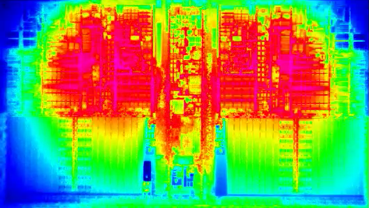
Chip designers care about both average and max chip temperatures. The average temperature is linked to leakage current loss, an optimization related to energy efficiency. But the max hotspot temperature is linked to chip failure. A design may target a maximum hotspot junction temperature of 105°C and an average junction temperature of 85°C; actual operating, throttling and shutdown thresholds are device-specific. Compute is limited as the relevant thermal threshold is reached.
A useful semiconductor-reliability rule of thumb is that every ~10°C increase in sustained junction temperature can roughly halve lifetime for a failure mechanism with an activation energy around 0.7 eV. That comes directly from the Arrhenius temperature-acceleration relationship used in semiconductor reliability qualification. JEDEC, for example, uses a 0.7 eV example in which 1,000 hours at 125°C corresponds to about nine years at 55°C.
Advanced chips can exhibit temperature differences of as much as 30°C across only a few hundred microns. As device dimensions continue to decrease and power maps become increasingly dynamic, these gradients can become important not only for thermal limits but for timing, leakage, reliability and power-delivery margins.
Effect of Hotspots
There are many distinct ways hotspots hurt an AI chip: an immediate performance/timing limit and a longer-term reliability limit. Usually the chip is throttled or designed around the hotspot well before it literally fails.
1. Temperature First Makes Transistors Slower
As junction temperature rises, carrier mobility generally decreases. Critical logic paths take longer to switch. So a chip designed to operate at a particular V,f can eventually reach a temperature where the critical path time is longer than the frequency interval and timing errors become possible.
Chip designers therefore leave thermal/timing margin or use temperature-dependent voltage/frequency controls. For an AI accelerator, a small 50–100µm hotspot can constrain the clock of a much larger block even though the average die temperature is acceptable.
This is an important reason hotspot temperature matters more than average temperature.
2. Leakage Increases Strongly with Temperature
Higher temperature generally increases transistor leakage, where in turn temperature again is driven by such leakage loss.
That positive feedback can become problematic at high temperature. Modern chips are designed to avoid true thermal runaway but leakage consumes an increasing fraction of the thermal budget and reduces the useful power available for computation.
Leakage loss is one of the dirty secrets of the chip industry. It exists and is big but no information about it is being shared by anyone. The industry’s secrecy about it results primarily just in the problem not being fundamentally addressed well.
3. SRAM Is Critical
For low-voltage chips, static random-access memory (SRAM) can become a critical constraint. SRAM operation depends on fairly small voltage/noise margins. Low voltage already makes all of this more difficult: read stability, writeability, noise margin, and process variation.
Temperature changes transistor characteristics and leakage and can further reduce operating margin. Therefore one can have the somewhat counterintuitive situation where the multiply-accumulate (MAC) arithmetic would happily continue operating but the nearby SRAM determines the allowable voltage/frequency/temperature operating point.
That makes localized SRAM temperature especially relevant to low-voltage AI accelerators.
4. Interconnect Reliability Gets Worse
Current density in advanced-chip interconnects is enormous. High temperature accelerates electromigration – metal atoms migrate under sustained current flow. A simplified Black’s-law relationship has mean time to failure (MTTF) decreasing with increasing current density and an exponential temperature dependence.
A hotspot therefore doesn’t merely heat the transistors underneath it. It also heats the power and signal interconnects carrying very high current into that region. Over time, electromigration can produce voids or hillocks, eventually causing increased resistance, opens, or shorts.
5. Dielectric and Transistor Aging Accelerate
Higher temperature accelerates several degradation mechanisms including:
- bias-temperature instability (BTI) shifts transistor threshold voltage over time.
- time-dependent dielectric breakdown (TDDB) eventually damages gate/interconnect dielectrics.
- hot-carrier degradation (HCI) can change transistor characteristics.
The details do not all have identical temperature dependencies but generally a chip operated hotter has less lifetime margin.
6. Thermal Gradients Create Mechanical Stress
This one is especially relevant to hotspots. Suppose most of the die is 70°C but a small region reaches 100°C.
The hotter silicon wants to expand more than its surroundings. That produces local mechanical stress. Repeated workload changes can create temperature cycles thousands or millions of times.
This thermal cycling can stress interfaces, BEOL structures, microbumps, hybrid bonds, underfill and package structures. In advanced 2.5D/3D packaging, those reliability issues become increasingly important.
Chip Lifetime Impact
Standard semiconductor reliability models explicitly show strong exponential temperature dependence for mechanisms including TDDB, BTI, EM and HCI.
Suppose a localized SRAM/compute region would otherwise run at 95°C, and near-junction Single Crystal Diamond (SCD) lowers it to 80°C while the rest of the chip changes little. For a 0.7 eV Arrhenius mechanism, that 15°C reduction corresponds to roughly a 2.5–3× improvement in temperature-driven lifetime of that hotspot region.
| Failure mechanism | Temperature sensitivity | Benefit from −20°C |
|---|---|---|
| Cu/interconnect electromigration | Very High | ~3–6× lifetime |
| TDDB / dielectric breakdown | High | ~2–5× |
| BTI transistor aging | High | ~2–4× |
| HBM cell/periphery degradation | Moderate-High | Potentially ~2–4× |
| SRAM marginality / timing failures | Strong operational benefit | Substantial |
| Thermal runaway / transient faults | Directly thermal | Potentially dramatic |
That does not mean that reducing hotspot temperature automatically triples the lifetime of an entire GPU. GPU lifetime depends on many components and failure mechanisms. The tables describe illustrative mechanism-level effects, not a qualified whole-chip lifetime guarantee.
For a representative mechanism with 0.7eV, the approximate impact is:
| Temperature increase | Remaining lifetime | If baseline life = 10 yrs |
|---|---|---|
| +5°C | 70–75% | 7–7.5 years |
| +10°C | 50–55% | 5–5.5 years |
| +20°C | 27–31% | 2.7–3.1 years |
| +30°C | 15–18% | 1.5–1.8 years |
The exact factor varies with the starting temperature. So, illustratively, if a particular wear-out mechanism had a 10-year MTTF (Mean Time To Failure) at 80°C, the same mechanism under otherwise identical stress would correspond approximately to: 5.3 years for 90°C; 2.9 years for 100°C; 1.6 years for 110°C.
This exponential temperature dependence is standard Arrhenius reliability behavior. NIST notes that activation energies vary substantially by failure mechanism, roughly from 0.3–0.4 eV to 1.5 eV or higher.
For electromigration, temperature has the same exponential character but current density factors in as well. So a hotspot can be doubly harmful: the hot compute/SRAM region is often also the region carrying high current density.
Or, more importantly for an accelerator vendor, instead of taking the longer lifetime, they can spend part of that reliability margin on higher allowable power, voltage, or frequency while maintaining the same target lifetime.
In other words, a 10–20°C hotspot reduction is not a small reliability improvement. Depending on the dominant failure mechanism, it can represent roughly a 2× to 4× change in modeled lifetime. That is one reason eliminating relatively small local temperature peaks can be economically meaningful even when the average chip temperature barely changes.
SCD substrating is technology we have developed to achieve Hotspots, Gone.