Twenty-five years of scientific pursuit have produced the first-ever single‑crystal diamond measuring 200mm in diameter.

At Diamond Foundry, we have created the first-ever D200mm single‑crystal diamond: one continuous crystal, 200mm in diameter. It marks a fundamental step forward in our ability to manufacture diamond as a technology material at semiconductor scale.
Diamond combines the highest thermal conductivity with exceptional mechanical strength, electrical insulation, optical properties, and the potential for extreme electronic performance. For decades, those properties have pointed toward new possibilities in technology. One basic limitation has stood in the way: size.
Why Scale Matters
The semiconductor industry is built around the ability to manufacture extraordinary materials at wafer scale. Silicon’s progression toward larger wafers transformed electronics by allowing increasingly sophisticated devices to be manufactured economically and repeatably.
Diamond has faced a different path. Natural diamond is constrained by geology, while conventional lab‑grown diamond has historically been constrained to relatively small crystal dimensions. As diamond’s properties became increasingly relevant to high‑power electronics, AI computing, optics, and quantum systems, crystal size remained a fundamental bottleneck.
Growing diamond at this scale required advances in plasma physics, reactor engineering, and process control.
Twenty-Five Years of Perseverance
The work behind this milestone began well before Diamond Foundry. Stefan Gsell and Martin Fischer have pursued the scientific and engineering challenge of growing high‑quality single‑crystal diamond of scalable size for 25 years. Stefan and Martin joined Diamond Foundry in 2022 through our acquisition of Augsburg Diamond Technology (Audiatec), bringing their crystal-growth expertise together with our reactor technology and manufacturing capabilities.
“This is one of those milestones that once seemed almost impossible,” said Martin Roscheisen, CEO of Diamond Foundry Inc. “Hundreds of DF engineers, scientists, and technicians contributed to us getting here. It is the accumulated result of countless experiments, failures, inventions, rebuilt machines, and insights over more than a decade.”
“Stefan and Martin pursued this goal for 25 years,” Roscheisen said. “There are very few examples in technology of someone sticking to a really hard scientific challenge with that level of perseverance. They kept going when the prevailing view was that single‑crystal diamond simply could not be made at this scale. Today, the perseverance shows as the first-ever D200mm single‑crystal diamond. And best of all, it makes D300mm predictable as well.”
That perseverance is reflected in advances across plasma generation, growth chemistry, reactor architecture, crystal engineering, thermal management, metrology, automation, and manufacturing.
What This Means for Computing
For us, D200mm is part of a broader effort to turn single‑crystal diamond from a scarce material measured in gemstones into a tech‑industrial semiconductor substrate manufactured at scale.
That matters as computing systems encounter increasingly severe thermal constraints. Modern AI processors concentrate enormous amounts of power into microscopic regions of silicon. Diamond’s exceptional thermal conductivity can spread that heat at the material level, creating new possibilities for chip architectures, power densities, reliability, and cooling.
A Beginning for Wafer‑Scale Diamond
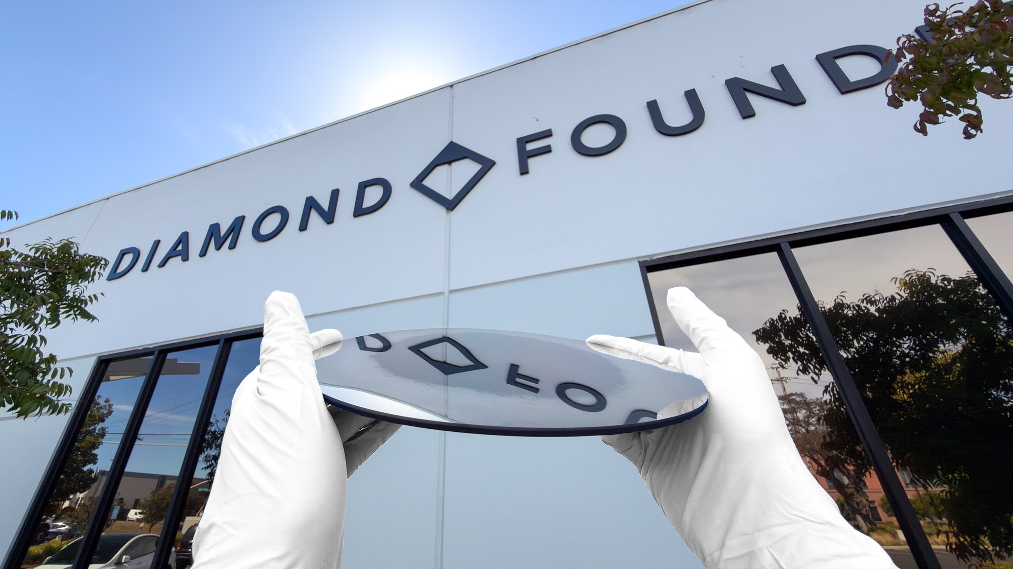
We are developing single‑crystal diamond for semiconductor and advanced‑technology applications where its combination of thermal, mechanical, electrical, and optical properties can enable performance beyond the limits of conventional materials. D200mm demonstrates a path beyond the size limitation that has held diamond back.
“Technology history is often written around the moment something finally works,” Roscheisen said. “But that moment rests on the people who were willing to spend years, sometimes decades, making it work. This diamond exists because hundreds of people contributed, and because a few people refused to give up on the idea for 25 years.”
Single‑crystal diamond has entered the wafer‑scale era.