3D Chip Thermal Solved with Edge Overhang Cooled Diamond Spacers
Chips packaged to place memory on top of the GPU in 3D enable much shorter wiring distances, resulting in distinct advantages in terms of performance (latency, memory bandwidth, etc.) and much – 6.7x according to TSMC – higher energy efficiency. The potential of true 3D is to avoid the energy lost in the long paths connecting compute and memory (which are far higher than just the Phy-to-Phy losses often cited when one properly includes the logic and GPU internal paths as well). Avoiding such energy loss not only saves energy but reduces heat management challenges in the first place.
But thermal challenges abound with 3D as HBMs are very sensitive to heat, and GPUs produce lots.
We describe the surprising discovery that a spacer between memory and compute made out of a single-crystal diamond (SCD) – one which overhangs the compute die by a few mm’s on each side and is cooled at such overhang only – is sufficient, even with standard cold plate cooling capacity, to solve the downside of heat concentration of 3D chip packaging.
Chip Packaging
In a CoWoS 2.5D world, compute dies and memory stacks are placed side by side on top of an interposer that provides the connectivity between them (with wiring longer than the chip size of close to 33x26mm). 3D packaging reduces interconnect delays and capacitance by placing memory on top of the logic. In addition, the reduced wire length significantly improves the energy needed to move data with I/O energy per bit improvements as high as 10x. But this is at the detriment of memory, which is heat-sensitive and now being effectively fried in the logic frying pan.
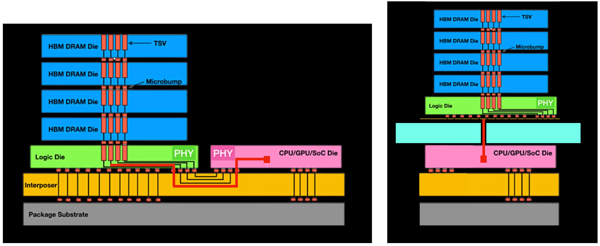
Figure 1: Moving from 2.5D (left) to true 3D (right) reduces wire lengths by as much as 10x. For a 10mm wide HBM and a 26mm wide GPU, while the Phy-to-Phy connection has been optimized to be very short, the path length can easily be 18mm in a 2.5D package whereas in a 3D package it can be less than 2mm even with a 1mm thick thermal spacer.
3D Chips with an Edge Overhang Cooled Diamond Spacer
Introducing a spacer made out of SCD with an edge overhang of several mm’s at which cooling is applied might be a simple solution to enabling 3D stacking.
Is cooling a diamond spacer at a slight overhang enough to cool an entire 3D chip package? SCD is obviously superb at thermal conductivity – see Appendix – but still, is this enough to provide benefit for an ASML reticle-limit sized chip packaged in 3D?
If the cooling is just connected to the edge face, it turns out not so – but if there is an overhang of several mm’s, it surprisingly turns out that yes, it is. (In a way, it evidences the >20x higher thermal conductivity of diamond vs silicon, which effectively allows heat to travel 20mm in diamond (half the chip size) when it would travel only 1mm in silicon.)
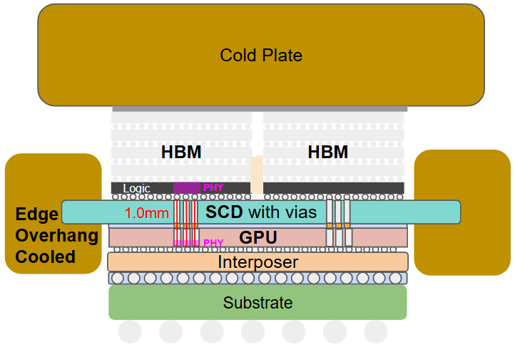
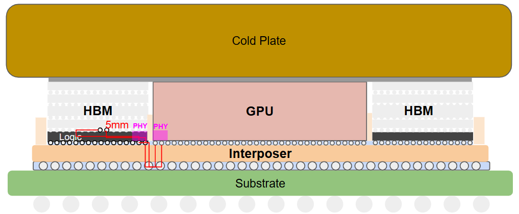
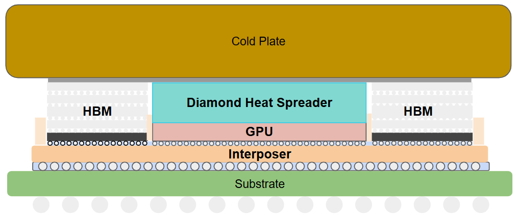
Figure 2: A 3D package with thru-vias SCD with edge overhang at which cooling is applied (top), a standard 2.5D CoWoS package with memory side-by-side the compute logic (middle), and a thermally optimized 2.5D package with thinned silicon and diamond heat spreader (bottom).
In other words, it turns out that SCD is so thermally conductive that it can laterally dissipate heat of ASML reticle limit-sized chips, provided there is an edge overhang that cooling can connect to. This overhang can be as little as a few mm’s on each side. (Indeed, there is negligible benefit to an overhang much larger than 5mm.)
Read all further in DF Tech Note 2512.